

Information Details
The Importance of Photomask Substrate in Semiconductor Production
Release time:
2023-04-27
Source:
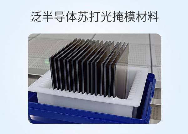
Mask technology plays a vital role in the field of semiconductor production. It can be used to make chips, shining light or electron beams into a photomask and projecting them onto a silicon wafer through a translucent film on the surface of the chip.photomask substrateIt is a special type of substrate that contains the precise lithographic patterns used to produce chips.
Photomask substrates are widely used in wafer fabrication processes because they provide highly accurate lithographic patterns for chip fabrication. This substrate is made of high-quality quartz material, and its surface flatness and flatness are very accurate, which can provide highly consistent and accurate scoring results. High-quality substrates can not only improve manufacturing efficiency and productivity, but also ensure the quality and reliability of the chip.
In semiconductor production, in order to ensure good manufacturing results, it is necessary to use a high-quality photomask substrate. Each substrate needs to undergo strict quality control to ensure that it meets the needs of the manufacturing process. These substrates are also specially treated to ensure that their surface is smooth and flawless, making it easier to perform photolithography. In addition, the substrates are also tested for performance to ensure that they can provide high-quality services during the manufacturing process.
photomask substrateIt is an integral part of the semiconductor production process. A high-quality substrate can ensure that the chip has a highly consistent and accurate scoring results, improve manufacturing efficiency and productivity, and ensure the quality and reliability of the chip.
In recent years, with the rapid development of microelectronics technology, the fabrication and application of photomask substrates has become one of the current research hotspots. So, what is a photomask substrate? Simply put, it is a series of tiny patterns that are used to make a template plate for miniature electronic devices. The fabrication and application of the photomask substrate will be described in detail below.
The manufacture of a photomask substrate is quite complicated, and its main steps include: making a photolithography mask, coating a photopolymerization agent, realizing pattern transfer by ultraviolet irradiation, and forming a photomask substrate after development. In the production process, it is necessary to strictly ensure the cleanliness of the operating environment, and at the same time use high-precision equipment for control.
photomask substrateWidely used in the semiconductor field, such as manufacturing integrated circuits, high-density memory devices, oscillators, etc., is one of the key tools for manufacturing microelectronic devices. In addition, there are also some applications in the fields of biomedicine and optics, such as the preparation of micro-optical fibers and biochips.
Compared with other microfabrication schemes, photomask substrates have higher accuracy and repeatability. In addition, its processing speed is faster and it can be mass-produced, so as to better meet the needs of industrial production.
The processing accuracy of the photomask substrate is affected by many factors, such as a lithography machine, a camera, a mirror and all other factors may cause errors. In addition, the selection and application of the photopolymerizable formulation is very critical.
Photomask substrate, photomask plate, reticle substrate
Latest News

05
2023
/
06