

Information Details
Application of photomask substrate in electronic field
Release time:
2023-05-12
Source:
photomask substrateIt is an important mold making material in semiconductor microelectronics manufacturing. It is a transparent or translucent material that can withstand high-resolution optical projection. Photomask substrates are widely used in the manufacturing process of semiconductor chips, flat panel displays, optical fiber communication devices, etc.
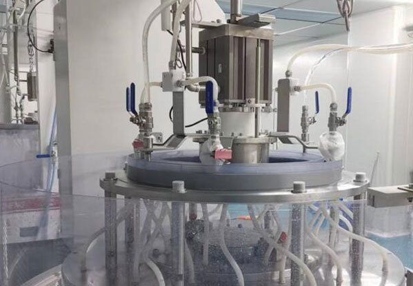
The material properties of the photomask substrate determine whether it can withstand high-resolution optical projection. Typical photomask substrate materials are glass, quartz, polymer, etc. For example, photoresist is a commonly used photomask substrate material. It has high optical transparency, chemical stability and mechanical strength, and is suitable for high-precision micro-processing. Production usually includes film graphics production, photoresist coating, exposure and development steps. Photolithography exposure light source is the key to the production of photoresist, the use of light source irradiation on the photomask, the formation of pre-selected patterns on the photomask, through the mask light transmission imaging, and projected onto the photoresist layer, to produce a tiny semiconductor device structure. The specific steps are cumbersome, and the conditions and parameters of different links need to be strictly controlled.
The photomask substrate is crucial in the manufacturing process of the semiconductor chip. It is mainly used in the parts related to the lithography process, including chip circuit design, mask production, optical equipment production, photoresist preparation, etc. In the fine processing of semiconductor chip manufacturing, the photomask substrate plays an extremely important role. In addition to applications in semiconductor chip fabrication, photomask substrates are also widely used in the fabrication of flat panel displays. A flat panel display is a grating optical instrument that refracts and reflects an initial beam in a specific order to form an image by printing and surface preparation of a photomask. Today's notebook computers, smart phones, flat panel displays and so on all use photomask substrates.
The photomask substrate is mainly used in the manufacture of an optical simulator when used in an optical fiber communication device. The optical simulator is an optical component that can simulate the optical properties of various optical fibers, and can simulate parameters such as transmission distance, optical fiber loss, concentration, distance and return loss. The application of the photomask substrate makes the optical simulator have more precise optical characteristics, and assists the optical fiber communication device to transmit data more stably. As the bottom material of semiconductor microelectronics manufacturing industry, photomask substrate is widely used in the manufacturing process of various small parts. It is believed that with the continuous development of science and technology, photomask substrates will also play a big role in more fields.
photomask substrateIt is a special semiconductor material substrate, which is widely used in the manufacturing process of microelectronic components. Once the substrate is made, it can be used for masking, photolithography, and other thin-film techniques in semiconductor chip manufacturing. Its main function is to provide a flat surface and stable reflectivity.
In the electronic manufacturing industry, the photomask substrate is a very important material. Because it has the following characteristics:
The photomask substrate can be manufactured with high precision, and can be manufactured with fine structure and wiring.
The photomask substrate is not easily corroded by chemicals and is not easily eroded by chemicals for processing, and is a relatively durable material.
During the photolithography process, the photomask substrate can maintain strong physical stability without deformation or deformation.
Therefore, photomask substrates play an important role in the fabrication of semiconductor chips and microelectronic devices. The emergence of this material has changed the manufacturing technology of the electronic manufacturing industry to a certain extent, making the process more accurate and stable.
Photomask substrate
Latest News

05
2023
/
06